 |
|
|
|
|
|
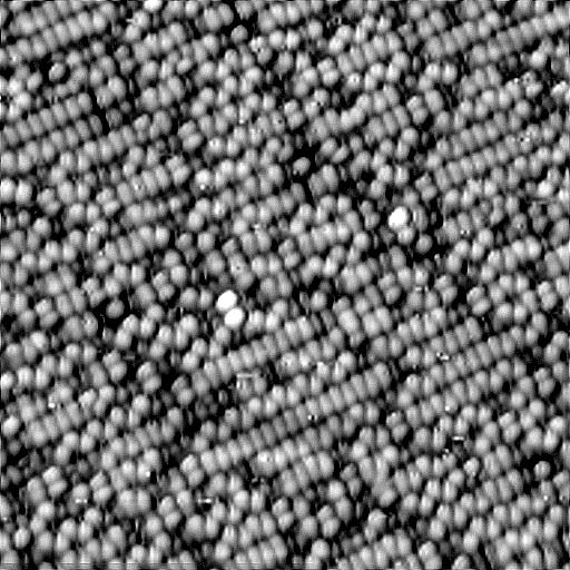
Si with 3% B |
||
See larger version of surface image above and a image created with Vistapro. |
|
This surface is a Si(001) surface exposed to boron. The sample bias voltage is -2.0 V, so filled states are being imaged and the change in surface structure caused by boron adsorption can be seen by comparing this image to the clean filled state image. In addition, you find a zigzag pattern, which is also clean Si dimers except these are the "buckled" dimers (asymmetric dimers). Other somewhat disordered regions are due to the boron species. Complex boron substitution mechanisms result in something called c(4x4) surface reconstruction, which shows as a diamond shaped structure. You need a good topographic view to see this diamond shape. 3-D is not the best way to view it. The RAW data file is 234 angstroms on a side. |
|
|
||
|
|
|
Fly-over movies |
|

|
Fly over the uneven surface. |

|
Explore at surface level. |

|
Take a mid-level tour of the surface set to music. |

|
This movie was rendered with a blue "sky" creating the impression of a journey through a strange desert of sand dunes. |
|
|
||
|
Vistapro surface file: 1081BSi.DEMFor directions on using Vistapro to view this surface see the Vistapro Lesson. |
||
|
|
||
|
Copyright © 1998 Division of Chemical Education Inc. of the American Chemical Society. All rights reserved. |
||